High-Brightness TFT LCD Engineering for Outdoor & Industrial HMI
·Senvita Display Engineering
High-brightness TFT LCD engineering addresses display systems that must remain readable in direct sunlight, high ambient light, or outdoor enclosures—typically 800–2500+ nits—with acceptable power, thermal, and lifetime tradeoffs.
This is not simply “order a brighter panel.” It is an optical, electrical, and mechanical co-design problem spanning backlight topology, driver headroom, thermal derating, and front-surface treatment. This pillar guide defines the engineering framework for outdoor kiosks, energy SCADA, rail HMI, marine bridges, and industrial sun-facing terminals.
What Is High-Brightness TFT LCD Engineering?
High-brightness industrial TFT LCD design is the discipline of achieving stable daylight-readable luminance while controlling:
- LED count, drive current, and optical extraction efficiency
- Power supply capacity and LED backlight power budgeting
- Thermal rise in sealed enclosures
- Color shift and luminance decay over 50k–70k+ hour service targets
- EMI from high-current switching backlight drivers
- Front glare vs contrast (anti-glare, AR coating, optical bonding)
Start from application lux targets, then derive nits—not the reverse. For baseline panel selection, see industrial TFT LCD selection.
Application Lux → Brightness Targets
| Environment | Ambient light | Typical target | Engineering notes |
|---|---|---|---|
| Indoor factory | 300–500 lux | 400–700 nits | Standard industrial HMI; cost-sensitive |
| Bright atrium / retail | 800–1500 lux | 700–1000 nits | May need AR coating |
| Outdoor shaded kiosk | 5000–10000 lux | 1000–1500 nits | Thermal and sealing critical |
| Direct sun readable | 30000+ lux | 1500–2500+ nits | Often requires optical bonding + high-power backlight |
Contrast ratio perceived by the operator depends on surface luminance difference, not panel nits alone. A 1000-nit panel with glossy cover can lose to a 700-nit optically bonded stack in real sun.
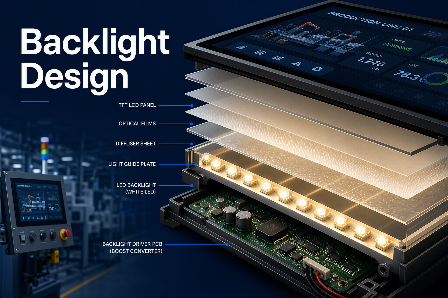
Backlight Engineering Stack
High brightness is achieved in the backlight subsystem—see backlight design for industrial TFT LCD for topology details.
Edge-lit vs direct-lit at high brightness
- Edge-lit: thinner, lower cost; brightness ceiling ~800–1200 nits typical without hot spots
- Direct-lit / matrix: higher peak nits, better local control; thicker, more thermal mass
Driver and power headroom
- Size LED driver IC for peak current + temperature derating, not room-temp datasheet max
- Separate analog dimming zone for high brightness to reduce PWM flicker (flicker analysis)
- Review LED driver ICs for current accuracy, PWM frequency range, and fault protection
Thermal Engineering
Every 100 nits above ~800 nits can significantly increase LED junction temperature in sealed boxes.
- Problem: brightness drops after 30 min sun soak → Cause: thermal derating → Solution: heat spreader to bezel, fan or vent path, reduce LED overdrive
- Problem: center hot spot → Cause: direct-lit density / LGP limitation → Solution: optical diffusion tuning or direct-lit zoning
- Problem: touch drift when hot → Cause: stack expansion / noise → Solution: bonding process control, touch firmware temperature comp
Wide-temperature qualification must include high-brightness soak: wide-temperature guide.
Optical Front Surface
- Anti-glare (AG): diffuses reflections; reduces sparkle in sun; may reduce crispness
- Anti-reflective (AR): reduces surface reflection; improves contrast in high ambient
- Optical bonding: eliminates air gap; major contrast gain outdoors; higher cost and rework complexity
Optical bonding is often mandatory above ~1200 nits in direct-sun applications—not optional industrial upsell.
EMI at High Backlight Power
Higher LED current increases di/dt on switching regulators. Architecture mitigations:
- Soft-switching or synchronized DC-DC where possible
- Keep backlight driver close to LED anode return; minimize loop area
- Validate conducted emissions with backlight at 100%—not 50% factory default
Cross-reference EMI troubleshooting and display subsystem architecture for grounding strategy.
Design Tradeoff Summary
| Goal | Engineering lever | Cost impact |
|---|---|---|
| +300 nits outdoors | LED overdrive + AR glass | Medium |
| Sun-readable 1500+ nits | Direct-lit + bonding + thermal path | High |
| Lower power at same nits | Efficient LGP / LED bin selection | Medium (NRE) |
| Longer lifetime | Run LEDs at 70–80% rated current | More LEDs / larger driver |
Validation Protocol
- Photometer: center and corner luminance at 25°C and max ambient soak temperature
- Sun simulator or outdoor A/B against reference UI screens
- 1000-hour accelerated aging at max brightness / max temp
- Power consumption at 100% white vs typical UI duty cycle
- EMC scan with backlight at full—not dimmed—power
Senvita High-Brightness Module Support
Senvita provides industrial TFT LCD modules from standard 500-nit indoor panels to high-brightness outdoor configurations with custom backlight, optical treatments, and LVDS or MIPI interfaces. Submit lux environment photos, enclosure drawings, input voltage, and target nits for an engineering RFQ.
Related articles: Backlight design, Wide temperature, Flicker analysis, TFT LCD selection.