MCU vs FPGA Display Interface Architecture
Part of: Display Subsystem Architecture for HMI
·Senvita Display Engineering
Choosing between an MCU-centric display path and an FPGA-based bridge is an architecture decision, not just a component choice. It affects boot time, signal integrity, update latency, software complexity, and the amount of debug effort required during bring-up. For the broader context, see Display Subsystem Architecture.
Definition
An MCU display architecture drives the panel directly, usually through RGB, SPI, parallel bus, or a simple bridge IC, with most timing and UI logic managed in software. An FPGA architecture inserts a programmable logic layer between the host and the panel, which is useful when the design must convert formats, buffer frames, replicate outputs, or enforce deterministic timing. A practical implementation often mixes both: the MCU handles application logic while the FPGA handles pixel timing and interface adaptation.
- Use an MCU when the panel bandwidth is modest and the UI update pattern is predictable.
- Use an FPGA when interface translation, frame buffering, or strict timing closure is the dominant problem.
- Consider pin count, memory topology, and firmware maintainability before choosing either path.
Problem: The UI stutters when multiple screens update at once.
Cause: The MCU is spending cycles on rendering, housekeeping, and protocol handling, so the display refresh path competes with application tasks.
Solution: Move timing-critical work into hardware, reduce frame churn, or add a small framebuffer/bridge layer that decouples rendering from scanout.
Problem: The board passes logic tests but fails with visible tearing or unstable sync.
Cause: The display interface is too close to the system load path, and firmware jitter changes the relative phase of write and scan operations.
Solution: Introduce deterministic buffering, lock the pixel clock path, and isolate display DMA or FPGA state machines from non-deterministic tasks.
Shijiaic has a practical bridge-design reference here: FPGA display bridge design.
Validation
Validation should prove both functional correctness and timing margin. Measure boot-to-first-image time, frame update latency, and worst-case refresh under CPU stress. Then inspect the physical interface.
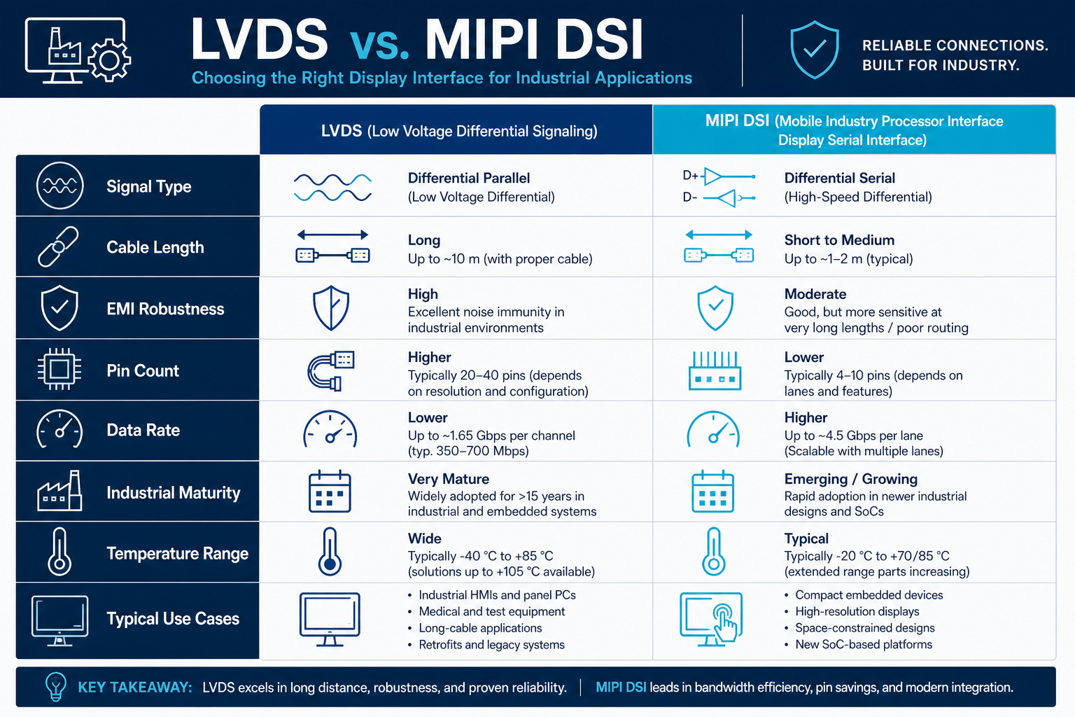
- Verify pixel clock tolerance, HSYNC/VSYNC stability, and lane mapping if a serializer is used.
- Run memory bandwidth stress tests while the UI animates to expose contention.
- Check signal quality at the connector and confirm that cable length does not collapse margin.
- Log reset behavior across cold boot, watchdog reset, and brownout recovery.
Related engineering notes: Touch Controller Integration in Industrial HMI, Industrial TFT LCD Connector Pinout Guide, EDID and EEPROM Configuration for Display Modules.